As electronic systems become smaller, faster, and more power-dense, packaging materials face increasingly demanding operating conditions. 5G communication equipment needs to manage heat generated by high-frequency power devices, electric drive systems in new energy vehicles must maintain stable operation at elevated temperatures, and space and satellite electronics may be exposed to wide temperature variations, vibration, and vacuum environments.
Under these conditions, conventional plastic packages may not always provide the combination of thermal performance, dimensional stability, and long-term reliability required by the application. Ceramic packages such as CLCC (Ceramic Leadless Chip Carrier) and CQFN (Ceramic Quad Flat No-leads) offer an alternative for electronic devices that require reliable surface-mount packaging together with better thermal and environmental performance.
1. What Are CLCC and CQFN Ceramic Packages?
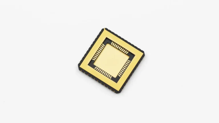
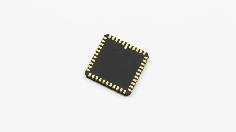
CLCC and CQFN are both leadless surface-mount packages based on ceramic substrates. Their metallized terminals are arranged along the four sides of the package, allowing them to be assembled directly onto a PCB using SMT processes.
Although they share a similar leadless, four-sided configuration, their internal structures are designed with different priorities.
CLCC: Ceramic Chip Carrier with a Cavity
CLCC is a ceramic chip carrier featuring a cavity that houses the semiconductor device. The cavity provides a stable physical environment for the chip and can be used for applications where long-term protection and package reliability are important.
Depending on the device design, the chip can be electrically connected through gold wire bonding inside the cavity or through flip-chip bonding.
The ceramic body also provides good dimensional stability and electrical insulation, making CLCC packages suitable for electronic devices operating under demanding environmental conditions.
CQFN: Leadless Package with a Thermal Pad
CQFN follows the leadless quad-flat package concept but incorporates a large exposed thermal pad on the bottom of the package.
This bottom pad provides a direct thermal path between the device and the PCB or cooling structure. It is particularly useful for devices that generate relatively high levels of heat while still requiring a compact four-sided surface-mount package.
The thermal-pad structure distinguishes CQFN from conventional leadless ceramic packages and makes it a practical option for applications where both compact packaging and thermal management are important.
2. Key Characteristics of Ceramic CLCC/CQFN Packages
Compared with conventional plastic packaging, ceramic packages offer a combination of electrical, thermal, mechanical, and environmental properties that can be valuable in high-reliability electronic systems.
High-Temperature Ceramic Materials
CLCC and CQFN packages can be manufactured using ceramic materials such as alumina (Al₂O₃) and aluminum nitride (AlN).
These materials provide electrical insulation and can maintain their physical and electrical properties under elevated temperatures and demanding environmental conditions. AlN can also provide higher thermal conductivity when thermal management is a major design consideration.
Leadless Four-Sided Surface-Mount Structure
The leadless configuration allows terminals to be arranged around the package footprint while keeping the package compact.
This structure supports:
- SMT assembly
- High-density PCB layouts
- Compact electronic designs
- Four-sided terminal configurations
Depending on the package design, different terminal structures and layouts can be used to meet the requirements of the electronic device.
Thermal and Electrical Performance
Ceramic materials are electrically insulating while offering thermal properties that can be useful for electronic packaging.
For applications involving high-frequency or higher-power devices, appropriate ceramic material selection and package design can help establish a controlled heat path while maintaining the required electrical insulation.
Precision Ceramic Manufacturing
Ceramic packages require controlled forming, sintering, machining, and metallization processes to achieve the required dimensional accuracy and terminal geometry.
A stable ceramic body and properly formed metallized pads are particularly important for surface-mount assembly, where package dimensions, flatness, and terminal consistency directly affect soldering and PCB integration.
Long-Term Reliability
The ceramic body and metallized terminals are designed to withstand the thermal, mechanical, and environmental conditions associated with the intended application.
Depending on material selection and package construction, ceramic packages can be considered for applications involving elevated temperature, humidity, vibration, and repeated temperature changes.
Different Terminal and Lead-Pitch Options
CLCC and CQFN packages can be designed with different terminal configurations to accommodate different PCB layouts and device requirements.
Available lead pitches can include 2.7 mm, 1.00 mm, and 0.50 mm, providing options for different package densities and interconnection requirements.
3. Where Are CLCC and CQFN Ceramic Packages Used?
CLCC and CQFN packages are commonly considered for integrated circuits and electronic devices where package reliability, electrical performance, thermal management, and compact SMT assembly are important.
Typical device applications include:
- Very-Large-Scale Integrated Circuits (VLSI)
Ceramic packages can provide a stable package structure for integrated circuits used in demanding electronic systems. - Application-Specific Integrated Circuits (ASICs)
CLCC and CQFN packages can be used for specialized ICs requiring compact surface-mount integration and controlled electrical and thermal characteristics. - High-Speed Emitter-Coupled Logic (ECL) Circuits
Ceramic packaging can support high-speed electronic designs where package structure and electrical characteristics are important considerations.
Beyond these device-level applications, ceramic packages are also used in several demanding system environments.
5G Communication Equipment
Power amplifiers used in 5G communication infrastructure, including devices based on GaN and LDMOS technologies, generate significant heat during operation.
Ceramic packages can provide electrical insulation and thermal management while maintaining a compact surface-mount footprint, making them suitable for selected high-frequency communication applications.
New Energy Vehicle Electronics
Electric drive systems in new energy vehicles operate under changing loads and elevated temperatures. Electronic components such as motor control units and power-related devices therefore require packaging that can maintain stable performance over extended operating periods.
Ceramic packages can be considered where temperature resistance, structural stability, and thermal performance are important packaging requirements.
Space and Satellite Electronics
Space and satellite electronics may operate under conditions involving large temperature variations, vacuum, and mechanical vibration.
The dimensional stability and environmental resistance of ceramic materials make CLCC and CQFN packages suitable for selected space electronics and satellite applications where long-term package reliability is an important consideration.
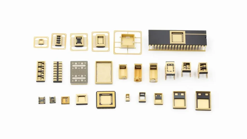
4. Other Ceramic Packaging Options from INNOVA Supplies
CLCC and CQFN are only part of the ceramic packaging solutions available from INNOVA Supplies. Depending on the device structure and application requirements, other ceramic package formats include:
- Laser SMD Ceramic Shells
- Surface-Mount Ceramic Power Packages
- Optical Communication Device Enclosures (ROSA/TOSA)
- Ceramic Dual In-Line Package (DIP) Enclosures
- Ceramic Small Outline Packages
These different package structures allow the ceramic material, package geometry, metallization, and mounting configuration to be selected according to the requirements of the electronic device.
INNOVA Supplies has launched several ceramic packaging enclosure products for electronic packaging applications. For technical specifications, samples, or application-specific requirements, please contact info@innovasupplies.com to discuss the available options.