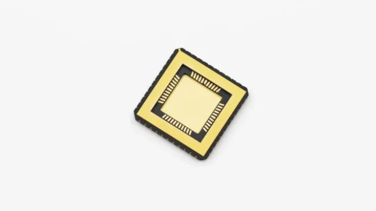
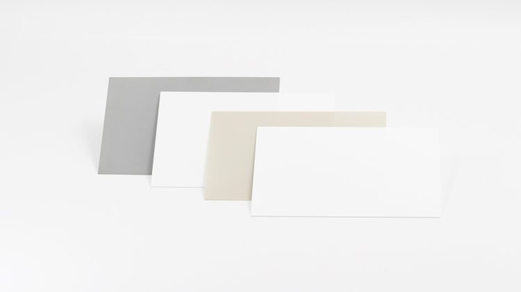
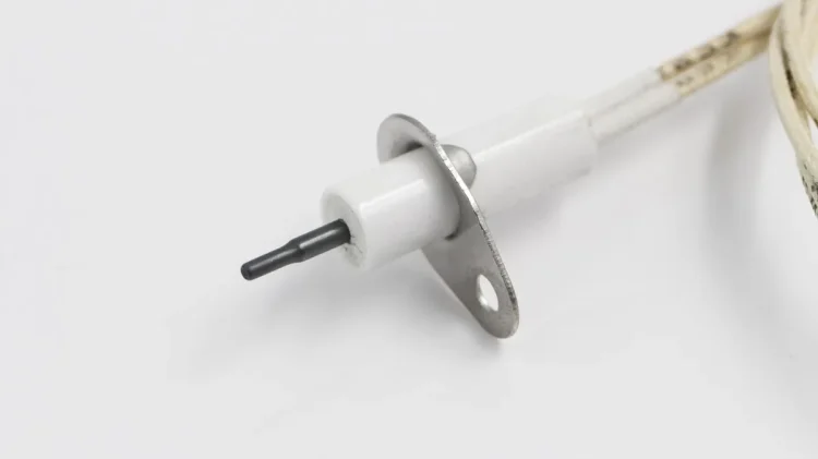
Aluminum nitride (AlN) ceramic substrates are widely considered for semiconductor packaging and power electronics because they combine electrical insulation with high thermal conductivity. As package power density continues to increase, AlN substrates can help provide an effective thermal path while maintaining the electrical isolation required by the device structure.
The challenge comes during machining. AlN is a hard and relatively brittle ceramic, making conventional mechanical dicing more difficult than processing many metal or polymer materials. Edge chipping, microcracks, tool wear, and frequent tool replacement can all affect processing consistency and production cost.
For this reason, laser processing has become an important approach for AlN substrate cutting and singulation, particularly for large-format ceramic panels.
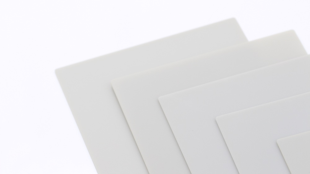
Laser Cutting for Large-Format AlN Panels
Large AlN mother panels, such as 138 × 190 mm sheets, are available in different thicknesses, with 0.5 mm and 0.635 mm being common options for certain applications.
Compared with mechanical dicing, laser cutting removes the need for direct mechanical contact between the cutting tool and ceramic substrate. This can help reduce mechanical stress during processing and provide better control over narrow cutting paths.
Two laser technologies commonly considered for AlN processing are:
- Ultraviolet (UV) lasers
- Picosecond ultrafast lasers
The appropriate laser source depends on factors such as substrate thickness, required kerf width, cutting speed, edge quality, and production volume.
Under suitable process conditions, laser processing can achieve dimensional accuracy within approximately ±10 µm. Ultrafast laser processing can also produce a relatively narrow heat-affected zone, helping to limit thermal damage and reduce the risk of residual microcracks around the cutting area.
Picosecond Laser Processing for 0.635 mm AlN
For relatively thick AlN substrates, such as 0.635 mm ceramic sheets, high-power picosecond lasers can be used to increase cutting efficiency while maintaining controlled edge quality.
For a 138 × 190 mm panel, cutting speeds of around 300 mm/min have been reported under specific processing conditions.
Actual cutting speed depends on several factors, including:
- Laser power and pulse characteristics
- AlN substrate thickness and material properties
- Cutting path and kerf requirements
- Required edge quality
- Number and depth of laser passes
- Equipment configuration and process optimization
Therefore, the reported speed should be treated as a reference for a particular laser setup rather than a universal processing rate.
Scribe-and-Break for Higher Throughput
Full-depth laser cutting is not the only option for AlN panel singulation. Scribe-and-break processing uses the laser to create a controlled partial-depth groove before mechanical separation.
Instead of removing the entire substrate thickness with the laser, the process creates a defined weakened line along the intended separation path. The panel can then be broken along the scribed area.
This approach can reduce laser processing time and, under suitable production conditions, may increase throughput by approximately 50% compared with a full-cut process.
The actual improvement depends on substrate thickness, laser parameters, scribe depth, panel layout, and the requirements for the final edge.
Flatness and Warpage: An Important Processing Variable
Large-format AlN panels introduce another practical challenge: flatness and warpage.
Thin ceramic substrates with relatively large dimensions may not remain perfectly flat across the entire panel. If the substrate surface changes in height during laser processing, the distance between the laser focus and the ceramic surface can also change.
Even a relatively small focal-position deviation can affect:
- Cutting depth
- Kerf consistency
- Edge quality
- Cutting stability
- Final singulation yield
For this reason, laser parameter optimization alone is not enough. Substrate fixturing, surface flatness, and focal-position control should also be considered when developing a production process for large AlN panels.
Key Factors in AlN Laser Singulation
For manufacturers evaluating laser cutting for AlN ceramic substrates, several process factors should be considered together:
| Factor | Main Consideration |
|---|---|
| Substrate size | Larger panels require more consistent positioning and flatness |
| Thickness | Thicker AlN generally requires greater processing energy or additional passes |
| Laser type | UV and picosecond lasers offer different processing characteristics |
| Cutting method | Full cutting and scribe-and-break have different throughput and edge-quality requirements |
| Focal control | Stable focus is important for consistent cutting depth and kerf quality |
| Fixturing | Proper support helps minimize movement and warpage during processing |
| Edge quality | Chipping and microcracks should be controlled according to the final application |
| Dimensional accuracy | Process parameters should be matched to the required substrate and package tolerances |
Improving the Singulation Process for AlN Substrates
As AlN substrates continue to be used in higher-power electronic packaging, efficient singulation becomes an important part of the overall manufacturing process.
Laser processing provides a non-contact alternative to conventional mechanical dicing and can offer advantages in dimensional control, tool wear, and processing flexibility. UV lasers, picosecond lasers, and scribe-and-break methods can each be considered according to substrate thickness, production requirements, and desired edge quality.
At the same time, successful AlN singulation depends on more than the laser itself. Panel flatness, fixturing, focal-position control, and process parameters all influence the final cutting quality and production yield.
For large AlN ceramic substrates, especially 138 × 190 mm panels in 0.5 mm or 0.635 mm thicknesses, selecting the appropriate cutting method and controlling these processing variables can help improve singulation consistency and production efficiency.