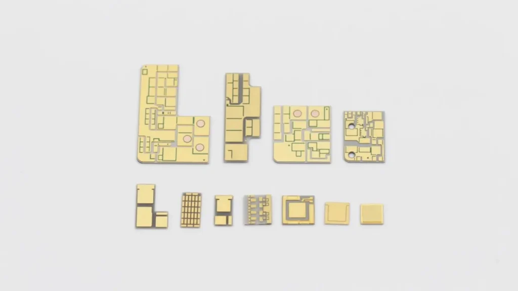
Ceramic substrates are extensively used in power electronics, LED packaging, and semiconductor devices because of their excellent electrical insulation, high thermal conductivity, and outstanding chemical stability. Despite these advantages, reliability issues can still arise during manufacturing and long-term operation. Among the most common failure modes are substrate cracking, warpage, and metallization failure.
In practice, these problems rarely originate from a single cause. Instead, they are usually the result of interactions among material characteristics, structural design, and process control.
I. Ceramic Substrate Cracking: A Typical Brittle Failure Mode
1. Common Failure Phenomena
Cracking of ceramic substrates is typically observed in the following situations:
- Cracks generated during machining or assembly
- Fracture occurring during reflow soldering or brazing processes
- Crack propagation during thermal cycling tests eventually leads to failure
2. Root Causes
(1) Thermal Expansion Mismatch
Ceramic materials such as Al₂O₃ and AlN have significantly different coefficients of thermal expansion compared with metals such as copper and gold. Repeated heating and cooling create thermal stresses at the interfaces, which often become the driving force for crack initiation and growth.
(2) Processing-Induced Surface Defects
Operations, including cutting, dicing, grinding, and drilling, can introduce microcracks or residual damage layers. Under subsequent thermal and mechanical loading, these defects may develop into larger cracks and eventually penetrate the substrate.
(3) Localized Stress Concentration
Sharp corners, insufficient edge clearance around holes, and abrupt changes in section geometry can all produce local stress concentrations, significantly reducing structural reliability.
3. Recommended Approaches
- Optimize component geometry to eliminate sharp corners and high-stress regions
- Improve machining quality to minimize microcracks and surface damage
- For high-reliability applications, consider ceramic systems with greater fracture toughness, such as replacing certain Al₂O₃ components with AlN where appropriate
II. Ceramic Substrate Warpage: Deformation Caused by Thermo-Mechanical Imbalance
1. Common Failure Phenomena
Warpage usually appears as overall bending or distortion of the substrate after sintering or subsequent processing.
Typical issues include:
- Insufficient flatness during SMT assembly
- Structural deformation after reflow soldering, resulting in non-uniform solder joint stresses
2. Primary Mechanisms
(1) Asymmetric Structural Design
In DBC, AMB, and other metallized ceramic structures, single-sided or asymmetric metal layers can create uneven thermal expansion constraints, leading to substrate warpage.
(2) Temperature Gradients and Differential Shrinkage During Sintering
Non-uniform furnace temperatures or poorly controlled heating and cooling rates can cause differences in densification behavior across the substrate, leaving residual stresses after sintering.
(3) Density and Microstructural Variations
Uneven green body density or localized porosity variations may produce inconsistent sintering shrinkage, ultimately resulting in macroscopic deformation.
(4) Metal Layer Thickness and Pattern Distribution
Particularly in DBC structures, copper thickness and pattern layout strongly influence warpage behavior and are often among the dominant contributing factors.
3. Recommended Approaches
- Adopt symmetrical metallization designs whenever possible
- Optimize sintering profiles to minimize temperature gradients and residual thermal stresses
- Improve the density uniformity of the ceramic body
- Carefully match copper thickness and circuit layout in DBC and AMB designs
III. Metallization Failure: The Combined Effect of Interface Degradation and Fatigue
1. Common Failure Phenomena
Metallization failures generally include:
- Local peeling or complete delamination of metal layers
- Pad failure or interruption of electrical pathways
- Reduced electrical connection reliability after thermal cycling
2. Primary Mechanisms
(1) Interfacial Bond Degradation
In DBC and AMB systems, bonding between ceramics and metals depends on reaction layers or transition layers formed at the interface. Insufficient or defective interfacial reactions can significantly reduce bond strength.
(2) Thermal Fatigue Accumulation
Because ceramics and metals expand at different rates, repeated thermal cycling continuously generates shear stress at the interface. Over time, stress accumulation can cause fatigue damage and eventual delamination.
(3) Process-Related Defects
Typical process defects include:
- Poor control of copper oxidation during the DBC process
- Inadequate wetting of active metals in the AMB process
- Voids or unbonded regions at the interface
- Non-uniform local interfacial reactions
3. Recommended Approaches
- Optimize DBC and AMB processing parameters to improve reaction uniformity
- Strictly control oxygen content and processing atmosphere, particularly during copper oxidation in DBC manufacturing
- Improve wetting and diffusion characteristics of the active brazing layer in AMB structures
- Conduct systematic thermal cycling reliability testing to verify long-term performance
IV. Key Factors Influencing Ceramic Substrate Reliability
In practical engineering applications, ceramic substrate reliability is generally determined by the combined influence of material selection, structural design, and manufacturing quality.
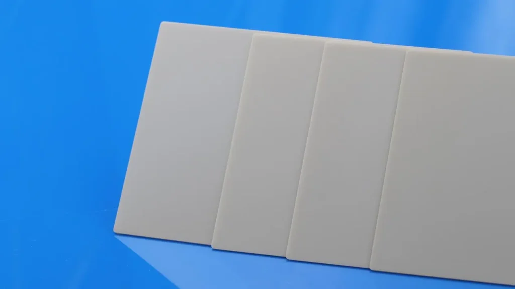
1. Material Selection
- Alumina (Al₂O₃): Mature technology with stable performance and relatively low cost
- Aluminum Nitride (AlN): High thermal conductivity, suitable for high-power-density applications
- Silicon Nitride (Si₃N₄): High strength and exceptional reliability for demanding operating environments
2. Structural Design
- Control of stress concentrations around holes, edges, and corners
- Copper layer distribution and structural symmetry
- Optimization of thermal and mechanical load paths
3. Manufacturing Process
- Uniform temperature control during sintering
- Reliable metallization interface quality
- Minimization of machining damage and optimization of post-processing techniques
V. Conclusion
Failures in ceramic substrates are seldom attributable to a single issue. More often, they result from the combined effects of material limitations, structural design decisions, and manufacturing process control.
For high-reliability applications such as IGBT power modules, SiC devices, and high-power LED packaging, reducing failure risks associated with thermo-mechanical coupling requires a systematic approach that integrates material selection, structural optimization, and robust process control.