As electronic devices continue moving toward higher power density, greater precision, and improved reliability, conventional substrate materials are facing increasing limitations. Issues such as insufficient thermal conductivity, poor stability at elevated temperatures, and limited surface precision have become major obstacles in the fabrication of advanced thick-film and thin-film circuits.
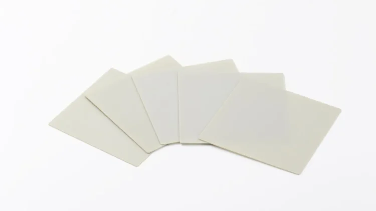
To support modern precision circuit manufacturing, substrate materials must provide a combination of reliable insulation, efficient thermal management, dimensional stability, and highly controlled surface quality. In this context, ceramic substrates have become an increasingly important solution for high-performance electronic applications.
Performance Requirements for Thick- and Thin-Film Circuits
Thick-film and thin-film technologies are both widely used in advanced electronic manufacturing, although their fabrication methods differ significantly. Despite these differences, both processes place strict demands on the substrate materials used as the circuit carrier.
Thick-Film Circuit Requirements
Thick-film circuits are typically produced by screen-printing conductive, resistive, or insulating pastes onto the substrate surface, followed by high-temperature sintering to form the final circuit structure. Sintering temperatures generally range from 850°C to 900°C, depending on the paste composition and process conditions.
During this process, the substrate must maintain excellent dimensional stability without deformation, warping, or shrinkage. It must also resist thermal shock and remain chemically stable to avoid reactions with the printed materials. At the same time, the substrate surface must provide suitable flatness and adhesion properties to support accurate printing.
Thin-Film Circuit Requirements
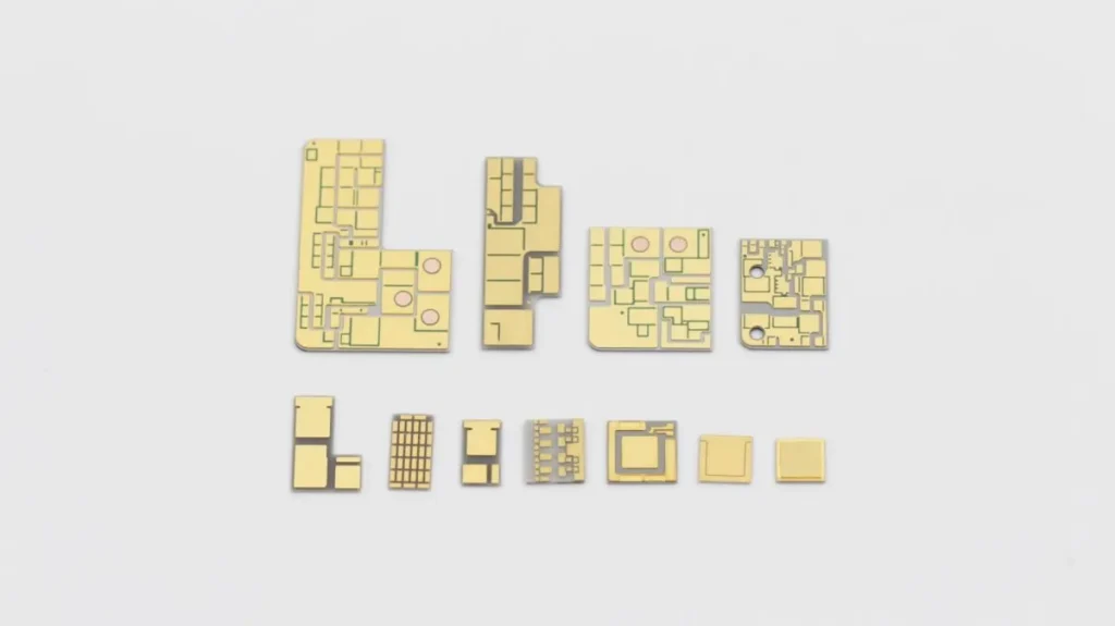
Thin-film circuits are manufactured using precision deposition, patterning, and processing technologies to create extremely fine conductive structures on the substrate surface.
For these applications, substrate surface quality becomes especially critical. The substrate must provide extremely low surface roughness and highly uniform microstructure to ensure precision pattern formation and minimize defects during manufacturing. High chemical purity is also essential to reduce contamination risks during controlled processing conditions.
Although thick-film and thin-film technologies use different manufacturing approaches, both require substrate materials with excellent thermal stability, dimensional consistency, chemical resistance, and controlled surface characteristics. Traditional organic or metal substrates often struggle to meet the requirements of advanced electronic applications.
How Ceramic Substrates Address These Challenges
1. Thermal Stability and Dimensional Reliability
Ceramic materials such as alumina (Al₂O₃) and aluminum nitride (AlN) offer high melting points and excellent thermal stability. They can maintain structural integrity during high-temperature thick-film sintering without softening or deformation.
This stability supports accurate multilayer circuit alignment, reduces thermal stress during processing, and improves long-term reliability. In addition, the thermal expansion characteristics of ceramic materials can be better matched with electronic components and conductive pastes, helping reduce thermal stress during operation.
2. Surface Quality and Precision Processing Capability
For thin-film circuits, ceramic substrates can be polished to extremely low surface roughness levels, supporting precise coating and fine-pattern manufacturing processes. For thick-film circuits, controlled surface texture can improve paste adhesion and printing consistency.
Through different surface treatment methods, ceramic substrates can be adapted to meet the specific requirements of various circuit fabrication processes.
3. Chemical Purity and Stability
Advanced ceramic materials feature high purity, dense microstructures, and excellent chemical stability under elevated-temperature and controlled processing conditions.
In thick-film processing, ceramic substrates remain stable when used with conductive paste systems. In precision circuit manufacturing, reduced volatile impurities help minimize contamination and process defects, contributing to improved manufacturing yield.
4. Thermal Management Capability
High thermal conductivity (AlN can reach 150–200 W/m·K) enables heat generated by electronic modules to dissipate efficiently, reducing local overheating and improving thermal reliability.
5. Mechanical Strength and Long-Term Durability
Ceramic substrates provide high hardness and flexural strength, helping reduce the risk of damage during processing, assembly, transportation, and long-term operation. Their resistance to thermal cycling, humidity, and corrosion also makes them suitable for demanding applications such as automotive electronics, industrial equipment, and advanced electrical systems.
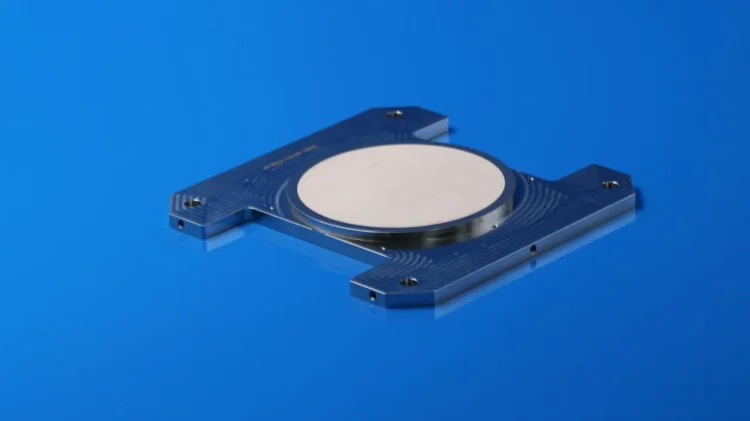
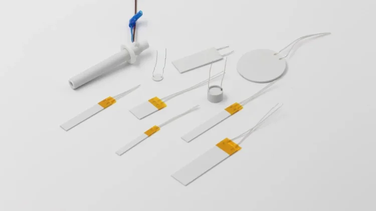
Overall, ceramic substrates provide a balanced combination of thermal, mechanical, chemical, and surface-performance advantages, making them highly suitable for thick-film and thin-film precision circuit applications.
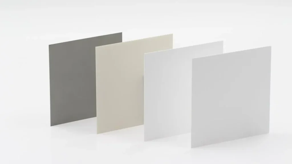
INNOVA Supplies provides multiple ceramic substrate material options to support a wide range of thick-film and thin-film circuit manufacturing requirements. For inquiries, please feel free to contact us.