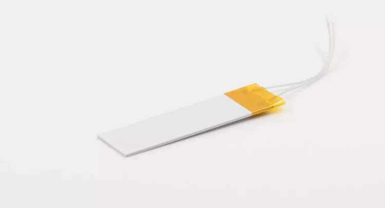
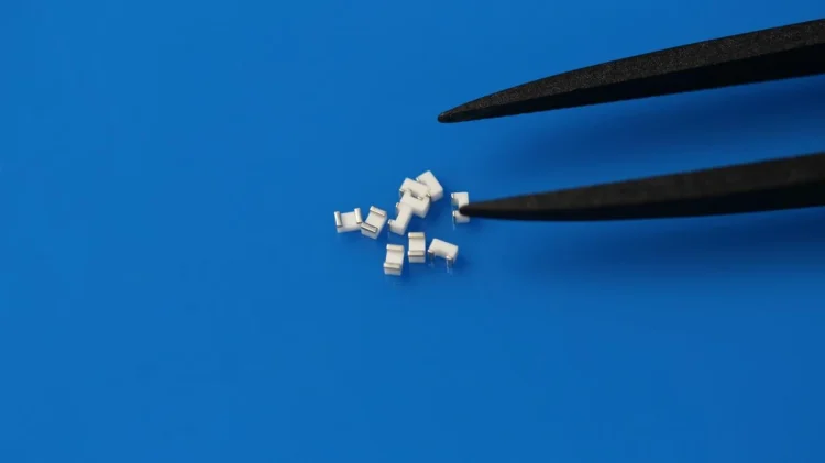
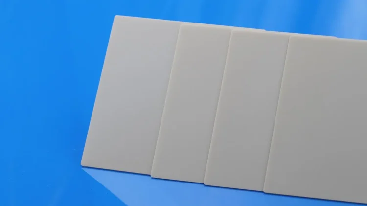
Ceramic substrates are used in electronic packaging as well as insulation and structural support components. For materials such as alumina (Al₂O₃) and aluminum nitride (AlN), substrate thickness can directly affect mechanical reliability, thermal management, electrical insulation, and processing stability.
The same applies to metallized structures such as DBC, DPC, and AMB. In these applications, the ceramic substrate must also accommodate thermal stresses from the metal layers. As a result, substrate thicknesses are usually based on established engineering requirements rather than selected arbitrarily.
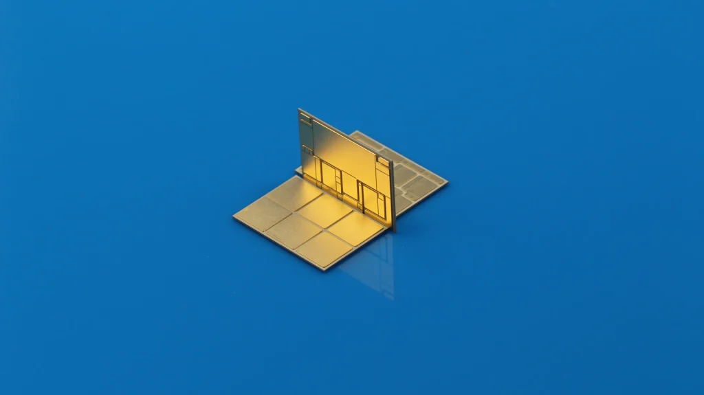
Silicon Nitride AMB Copper-Clad Substrate
I. Why Is Ceramic Substrate Thickness Important?
Ceramics are hard and rigid but relatively brittle, making thickness an important consideration during processing and application.
Thickness selection is mainly affected by:
- Mechanical strength and bending resistance
- Thermal conductivity and heat dissipation
- Electrical insulation requirements
- Stress matching with metallization or packaging structures
- Processing capability and production yield
- Final assembly dimensions
An overly thin substrate may have a higher risk of cracking and warpage, while excessive thickness can increase thermal resistance and processing costs. Non-standard thicknesses may also make cutting, metallization, and subsequent packaging more difficult to control.
For DBC and DPC structures, the substrate must withstand the thermal stress associated with copper layers and repeated temperature changes. Therefore, thickness needs to be considered together with the material and metallization structure.
II. Ceramic Substrate Thickness by Application
1. Electronic Packaging and Power Modules
Metallized ceramic substrates used in DBC, DPC, and AMB structures are commonly found in power electronics, semiconductor modules, and industrial electronic equipment.
The substrate needs to provide electrical insulation, support the metal layers, assist thermal management, and maintain structural stability during thermal cycling. For this reason, commonly established thickness specifications are generally preferred to achieve a balance between mechanical strength, thermal performance, and manufacturing stability.
2. Industrial Structural and Insulation Applications
Ceramic substrates are also used without metallization in applications such as:
- Insulation components for semiconductor equipment
- High-temperature support and positioning parts
- Vacuum and plasma equipment
- High-voltage insulation structures
- Precision mechanical support components
In these applications, thickness is mainly determined by requirements for rigidity, dimensional stability, insulation distance, and environmental resistance.
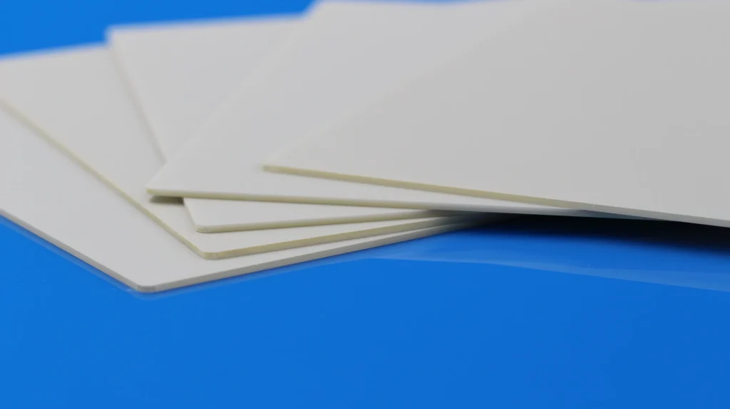
Aluminum Nitride Substrate
III. Common Ceramic Substrate Thickness Ranges
Although ceramic substrates are available in various thicknesses, industrial applications tend to concentrate around several established ranges.
1. Thin Precision Structures: 0.25–0.5 mm
This range is mainly used for compact and lightweight structures, including high-frequency electronics, miniaturized packaging, and precision components.
Because the substrates are relatively thin, material consistency, dimensional accuracy, warpage control, and handling require greater attention.
2. Main Industrial Range: 0.5–0.635 mm
0.5 mm and 0.635 mm are common engineering specifications used in power electronics, industrial electronics, and sensor structures.
This range provides a practical balance between structural stability, thermal performance, and processing efficiency.
3. Higher-Strength Structures: Around 1.0 mm
Substrates around 1.0 mm thick are often used where greater rigidity and structural stability are required, such as power modules and industrial equipment.
Compared with thinner substrates, they provide stronger mechanical support, although the increased thickness also needs to be considered in thermal design.
4. Reinforced and Special Structures: 1.2–1.5 mm
The 1.2–1.5 mm range is generally used for heavier-duty structures and special industrial applications requiring greater rigidity and impact resistance.
The increased thickness can improve structural stability but may also increase processing costs and affect the thermal path.
IV. Ceramic Substrate Materials and Specifications
INNOVA Supplies can provide ceramic substrates in different materials, dimensions, thicknesses, and surface roughness specifications to meet requirements for insulation, thermal conductivity, and structural strength.
Available materials include Al₂O₃, ZTA, AlN, and Si₃N₄, with typical specifications shown below:
| Parameter | Unit | Al₂O₃ | ZTA | AlN | Si₃N₄ |
|---|---|---|---|---|---|
| Effective Dimensions (A, B) | mm | 50.8–190 | 50.8–190 | 50.8–190 | 138 × 190 |
| Thickness (T) | mm | 0.25–1.5 | 0.25–1.5 | 0.25–1.0 | 0.25, 0.32 |
| Thickness Tolerance | mm | ±5% (min. ±0.03 mm) | — | — | — |
| Warpage (C) | mm | ≤0.3% | — | — | — |
| Surface Roughness | μm | 0.2–0.6 | 0.2–0.5 | 0.2–0.75 | 0.2–0.75 |
Size, thickness, and surface roughness can be adjusted according to specific application requirements.
If you need to evaluate material selection, substrate dimensions, thickness, surface finish, or other structural requirements, please get in touch with the INNOVA Supplies team for further technical support and product information.