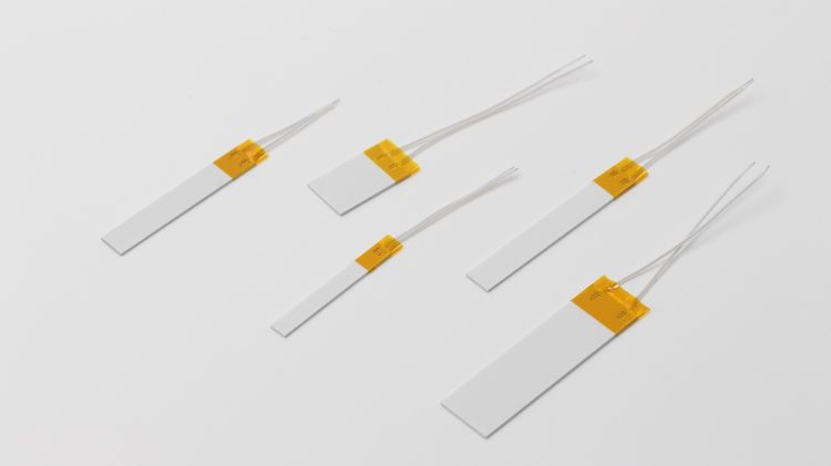
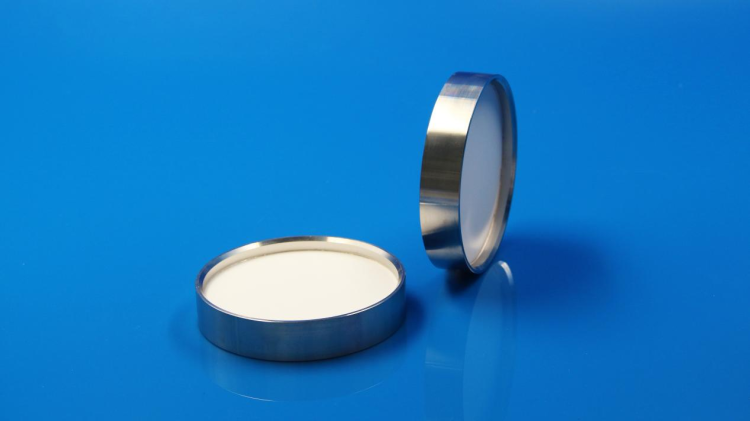
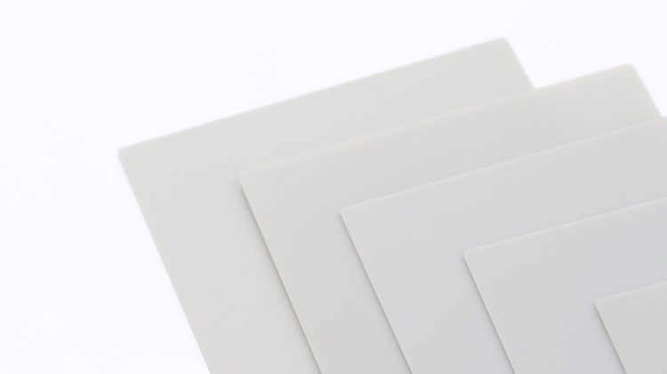
When selecting aluminum nitride (AlN) ceramic substrates for power electronics and electronic packaging, thickness is an important design consideration. Both 0.635 mm and 1.0 mm are commonly used options for substrates processed through metallization technologies such as DPC, DBC, and AMB.
For a standard 138 × 190 mm mother panel used in subsequent dicing and component fabrication, thickness affects more than thermal performance. It also influences substrate rigidity, warpage, and the way mechanical stress develops during bonding and thermal cycling.
In some projects, the initial thermal design may meet its requirements, yet problems such as increased warpage, interfacial delamination, or failures during thermal cycling can still occur later in production. These issues do not necessarily indicate poor material quality. In many cases, they are related to how substrate thickness interacts with the metallization structure, assembly process, and operating conditions.
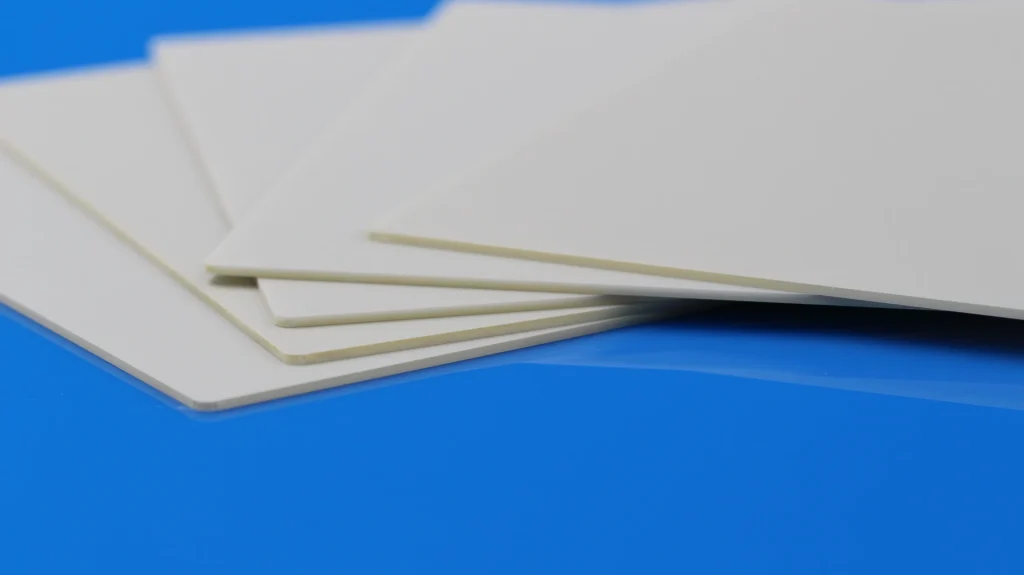
Aluminum Nitride Substrate
1. How Substrate Thickness Affects Thermal Performance and Rigidity
AlN substrate thickness influences both heat transfer and mechanical stiffness, so the choice involves balancing thermal response against structural stability.
A 0.635 mm AlN substrate provides a thinner heat transfer path and may suit compact power assemblies where thermal response and high integration density are important. However, its lower bending stiffness makes it more susceptible to deformation under uneven bonding pressure, residual stress, or stress generated by metallization layers.
A 1.0 mm AlN substrate provides greater mechanical rigidity, helping the panel resist deformation during manufacturing, bonding, and repeated heating cycles. This can be beneficial when structural stability is a priority. However, the additional thickness increases the distance through which heat must travel, which may affect thermal response depending on the overall assembly design.
The two thicknesses therefore serve different design priorities. Neither is automatically better in every application; the appropriate choice depends on the thermal and mechanical requirements of the complete structure.
2. Common Problems During DPC, DBC, and AMB Processing
During DPC, DBC, and AMB manufacturing, thickness-related issues may appear as local delamination, uneven stress across the metallization layers, or increased deformation after thermal cycling rather than as obvious defects in the ceramic material itself.
A substrate may meet its material specifications while the assembled structure still experiences reliability problems. This can happen when thickness selection is made without fully accounting for the following factors:
- Metallization structure: Copper layer thickness and the arrangement of multiple layers affect stress distribution.
- Bonding pressure and tooling: Uneven pressure or unsuitable fixtures can contribute to deformation.
- Thermal cycling conditions: The temperature range and number of cycles influence accumulated stress.
- Circuit pattern layout: Pattern density and copper distribution affect local stress and structural balance.
- Warpage tolerance: The allowable deformation must be defined according to downstream processing and assembly requirements.
These factors should be evaluated together. Choosing a substrate based on thickness alone may not provide sufficient control over the stability of the final assembly.
3. When to Choose 0.635 mm or 1.0 mm AlN Substrates
In general, 0.635 mm AlN substrates are worth considering when compact packaging, high integration density, and thermal response are key priorities. 1.0 mm AlN substrates may be more suitable when greater substrate rigidity and dimensional stability are needed.
For 138 × 190 mm panels, the effects of thickness can become more noticeable because the large panel area makes flatness, support conditions, and stress distribution particularly important. The final result depends not only on the ceramic thickness but also on the metallization design, processing conditions, and assembly structure.
The selection should therefore be based on the requirements of the intended application rather than assuming that a thinner or thicker substrate will always deliver better performance.
4. Practical Considerations Before Finalizing Thickness
Before sample validation or mass production, it is advisable to evaluate substrate thickness alongside the actual processing and assembly conditions.
Key information to establish includes:
- The metallization process: DPC, DBC, or AMB
- Copper layer thickness and overall layer structure
- Bonding pressure and tooling arrangement
- Thermal cycling conditions and reliability requirements
- Circuit pattern density and layout constraints
Together, these parameters help establish a suitable thickness range and reduce the risk of deformation or interfacial problems in later production stages.
AlN Ceramic Substrates from INNOVA Supplies
INNOVA Supplies offers large-format aluminum nitride ceramic substrates in 138 × 190 mm, with common thickness options including 0.635 mm and 1.0 mm. These substrates can serve as base materials for DPC, DBC, AMB, and other downstream precision processing applications.
Different substrate specifications can be considered according to application requirements, structural design, and process development needs.
For product information, specification inquiries, or assistance identifying suitable substrate options, contact info@innovasupplies.com.