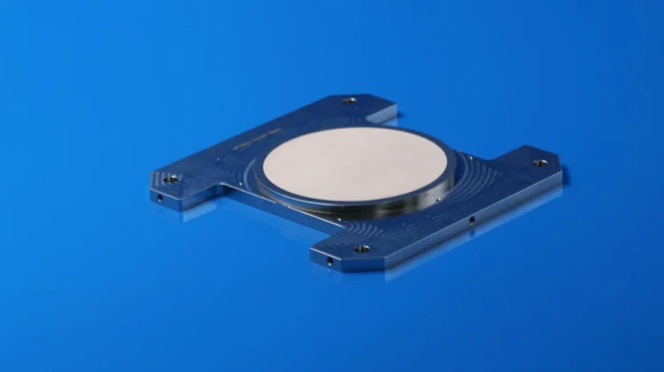
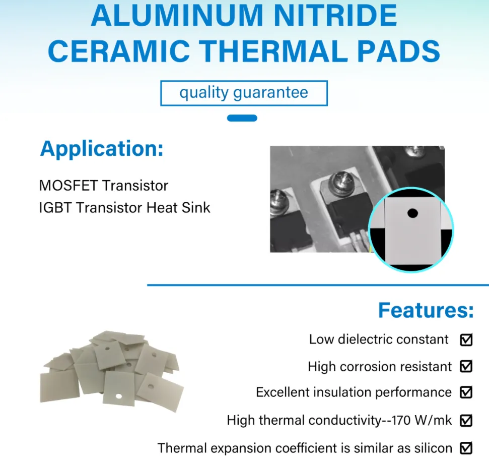
INNOVA Suppplies ceramic interface pads solve a fundamental problem: they create reliable thermal pathways between hot components (like power transistors) and their heat sinks, eliminating pesky air gaps caused by imperfect surfaces. Forget thermal bottlenecks – we fill those microscopic valleys efficiently.
- TO-3P-220-247-254-257-258-264_Aluminum_Nitride_Ceramic_Thermal_Pads
Why Ceramic? Especially AlN?
We use two workhorse materials: alumina (Al₂O₃) and aluminum nitride (AlN). Here’s why they’re special:
AlN is the star performer: Its thermal conductivity blows alumina out of the water (we’re talking 7-10× better!).
Stays cool electrically: Top-tier insulation even under high voltage – no leakage, no breakdown.
Built tough: Handles crazy temperature swings (-50°C to 500°C+), laughs at corrosion, and won’t crack under stress.
Plays nice with silicon: Matches silicon’s expansion rate, so no stress cracks in your chips.
Silent partner: Zero noise, and crucially, no parasitic capacitance messing with your MOSFET/IGBT gates.
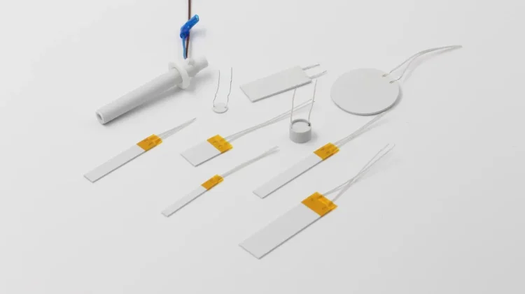
Where You’ll Use Them:
Perfect for:
Power devices (MOSFETs, IGBTs – you name it)
IC packaging thermal management
Heat sink interfacing
LED board TIM applications
COF (Chip-on-Film) cooling
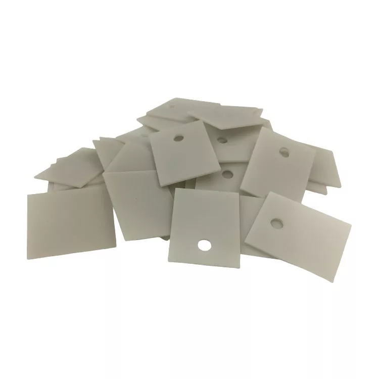
Our Go-To: Aluminum Nitride Pads (No-Hole Design)
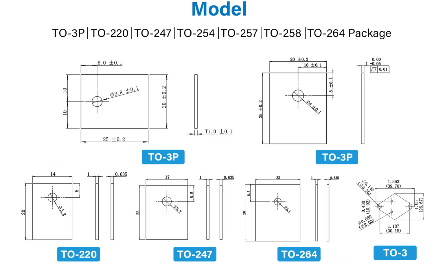
We stock AlN pads tailored for TO packages like:
TO-3P, TO-220, TO-247, TO-264, TO-3, TO-254, TO-257, TO-258
(Need holes? We do those too – just ask.)
Installation – Quick & Solid:
Prep surfaces: Clean both components thoroughly. Align the pad.
Stick the power device: Mount your transistor/MOSFET onto the pad.
Screw down: Secure the stack (device + pad + heatsink) with screws. Done.
Sizes We Keep On Hand:
Here are common dimensions (thickness typically starts at 1mm – custom thickness available):
TO Package Dimensions (L × W mm) Notes
TO-3P 25 × 20
TO-220 20 × 14
TO-247 22 × 17 Often 0.635mm thick
TO-264 28 × 22
TO-3 39.7 × 26.67 Diamond shape
TO-254 34 × 24
TO-257 40 × 28
TO-258 50.8 × 50.8 Square
Also standard sizes: 25.4×25.4, 114.3×114.3, 152×152, 190.5×138mm.
Custom cuts? Absolutely – send us your drawing.
Regular Size Drawing:
- TO-3P 220 247 254 257 258 264 Aluminum Nitride Ceramic Thermal Pads For MOSFET Transistor IGBT Transistor Heat Sink
(Visual: Schematic showing pad mounting on typical TO-packaged MOSFET/IGBT)
- TO-3P 220 247 254 257 258 264 Aluminum Nitride Ceramic Thermal Pads For MOSFET Transistor IGBT Transistor Heat Sink
Our Quality Standards – No Compromises:
Parameter Requirement Why It Matters
Thickness ±0.01mm (per your spec), Consistency in thermal stack
Flatness ≤ 0.01mm eliminates air pockets
Camber (Warp) ≤ 0.2% Ensures even pressure
Surface Finish Ra ≤ 0.5µm Smooth contact surface
Visuals Flawless – no chips, cracks, or stains. Reliability first
Cleaning Ultrasonic + alcohol wash, baked dry no residues, no watermarks
Handling Packed in ESD-safe pearl foam immediately prevents shipping damage
How We Pack Your AlN Pads:
Clean & dry: Every piece is ultrasonically cleaned, alcohol-rinsed, and baked dry.
Safe storage: Placed in partitioned pearl foam trays – 100pcs per cell.
Boxed smart: 5 cells per box (500pcs total), shrink-wrapped with a clear specs label.
Ship securely: Boxes go into reinforced cartons (21×21×12cm, ~1.5kg).