Product Properties
Downloads & Resources
| Resource Type | Link |
|---|---|
| Technical Data Sheet (TDS) | 20-Pressureless Sintering Silicon Carbide Ceramic Material Properties-SU0002 |
Product Details
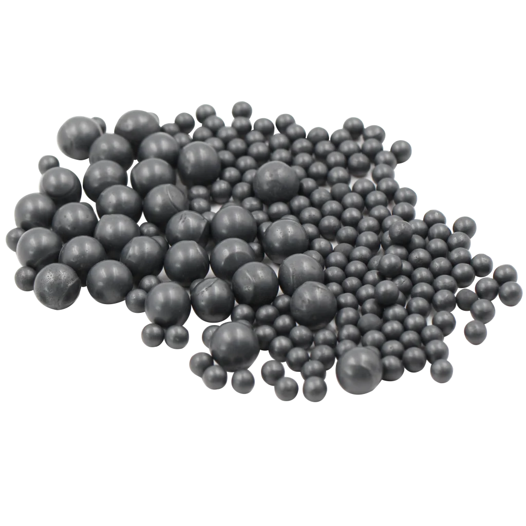
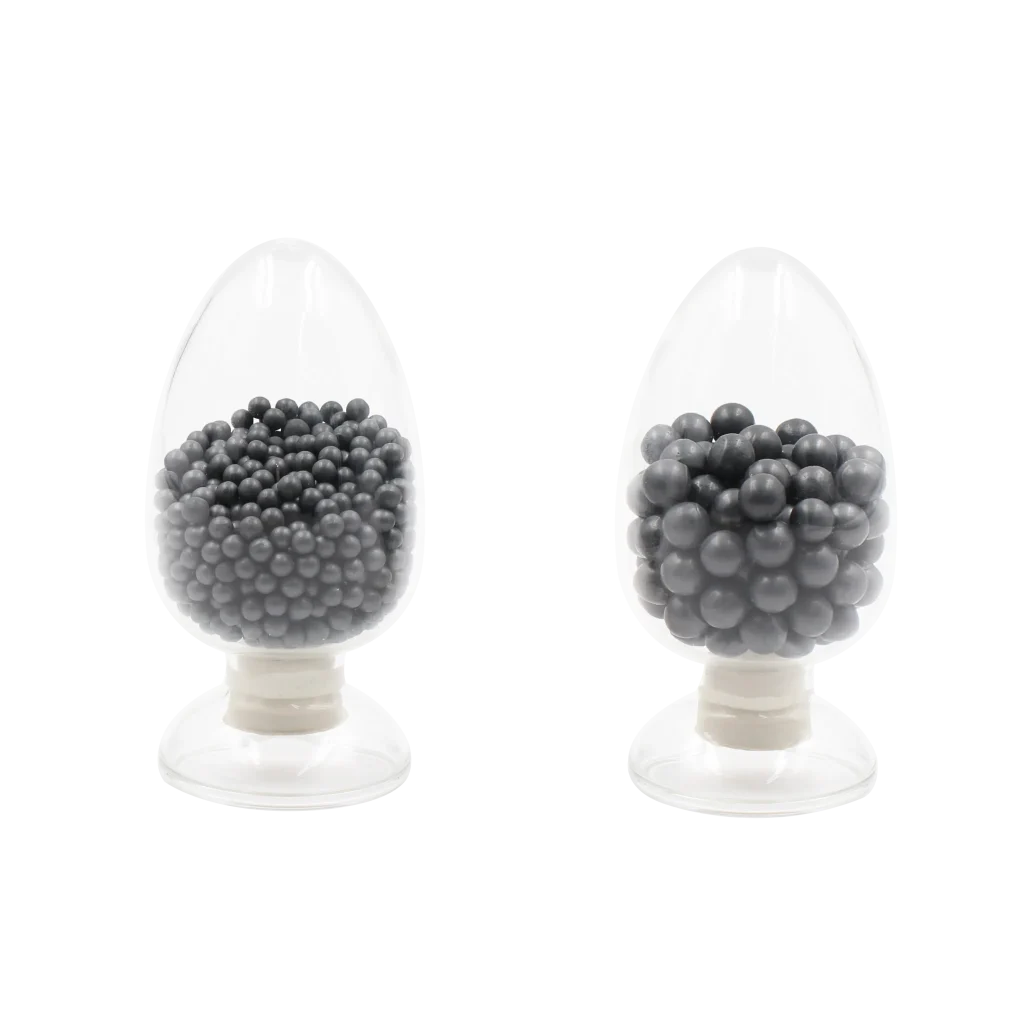
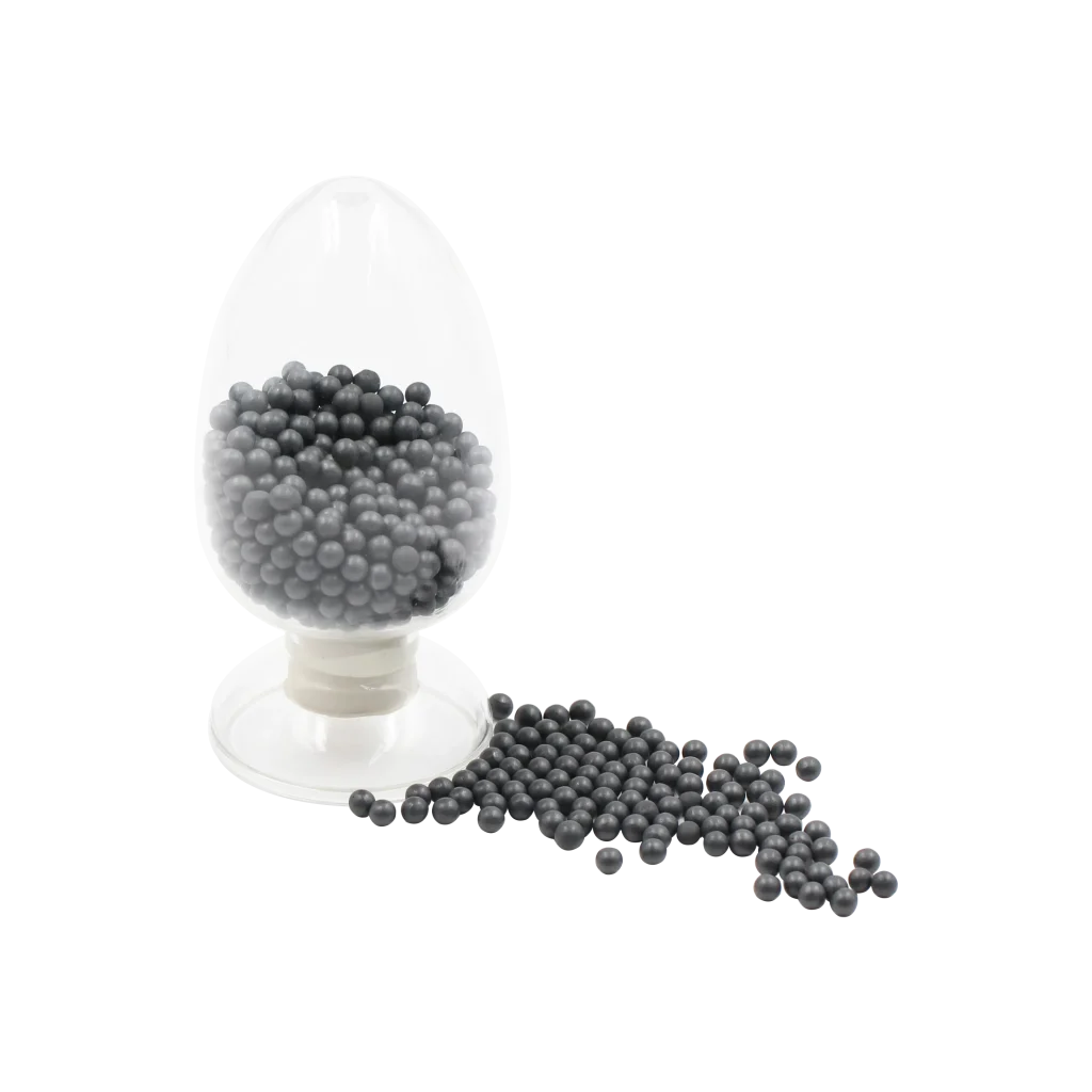
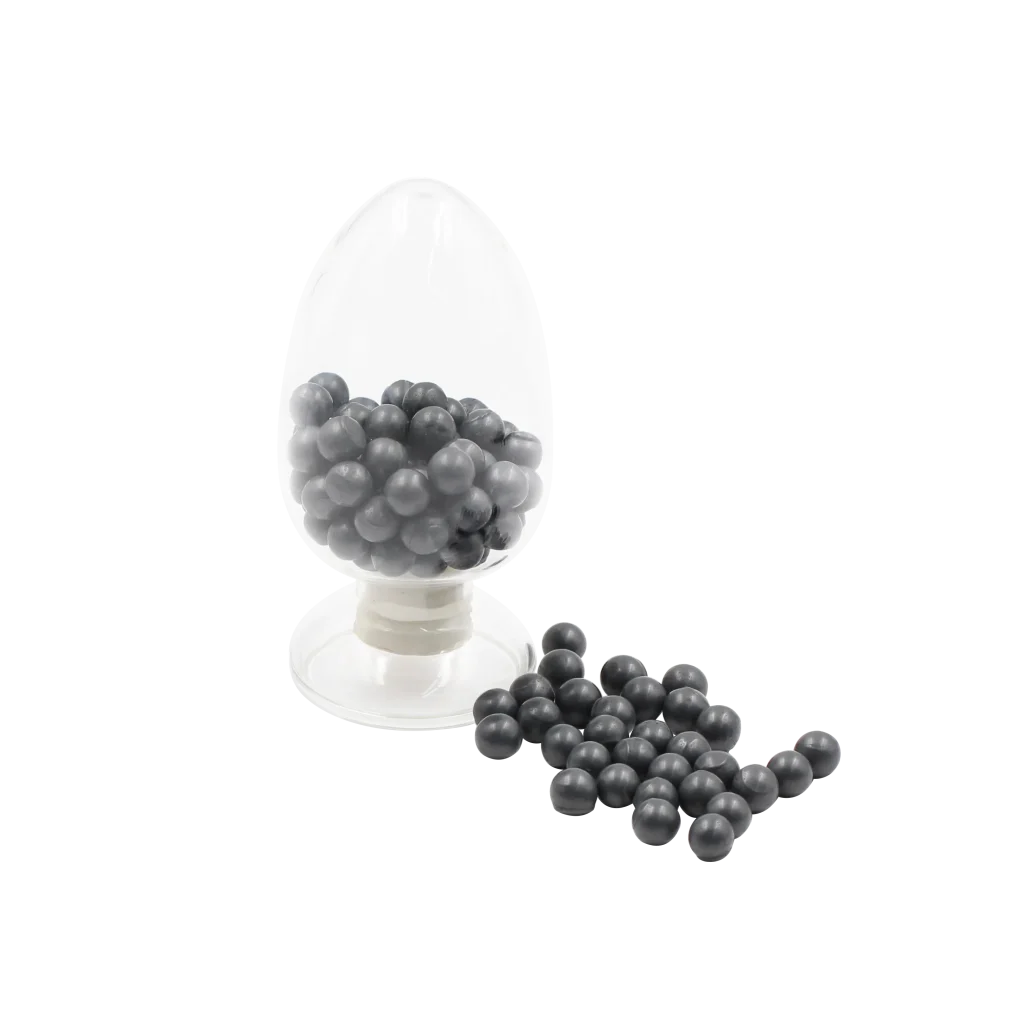
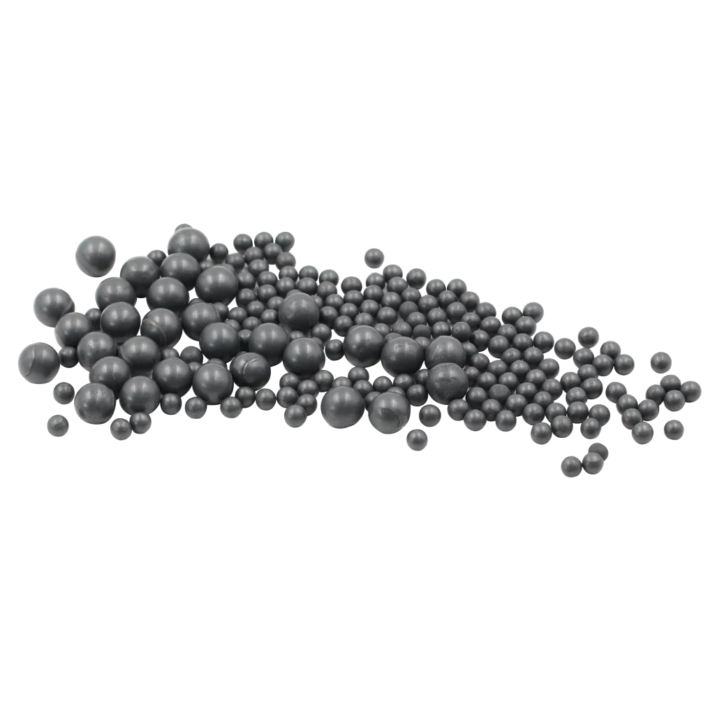
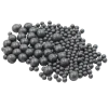
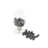
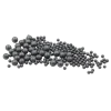
Silicon carbide grinding media ball has unique features such as high strength, good wear/corrosion/chemical resistance, light weight, low thermal expansion, high temperature resistance, electrical insulation, and non-magnetic. It is perfect for grinding application that requires high temperature, high hardness, and minimized contamination, such as semiconductor and electronic coating. Its high hardness can meet the vast majority of metal powder crushing and refining. They are extensively applied in the fields of Metallurgy, Ceramics, Electronics, Light Industry, Paint, Medicine, Geology, Chemical Engineering, and so on.
Our silicon carbide balls possess good wearability, a low thermal expansion coefficient, extreme corrosion resistance, high hardness, and self-lubricating properties.
Silicon Carbide Ceramic Grinding Balls Feature
- Excellent abrasion resistance
- High purity
- Excellent corrosion resistance
- Energy saving of grinding and dispersion
Silicon Carbide Ceramic Grinding Balls Applications
- Engineering Ceramics
- Enamel
- Glass
- Chemicals
| SIC | ≥99% |
|---|---|
| Color | Black |
| Specific Density | ≥ 3.1 g/cm³ |
| Flexural strength | ≥400 Mpa |
| Compressive Strength | ≥ 2200 Mpa |
| Indicated Parosity | < 0.2% |
| Coefficient of Heat Expansion | 40(10-6.1/°C) |
| Thermal Conductivity | 90-110 W/m.k |
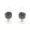
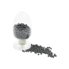
Stock size: 5mm、10mm
Surface treatment: Unpolished
Frequently Asked Questions
Silicon carbide (chemical formula: SiC) is a non-metallic carbide formed by the covalent bonding of silicon and carbon elements. It has various crystal forms, such as α (hexagonal) and β (cubic). It is the hardest material in nature after diamond and cubic boron nitride, with a Mohs hardness of 9.2-9.5. It is also an important power semiconductor substrate, high-temperature refractory material in modern industry.
Silicon carbide does exist in its natural form in nature, but it is scarce. Its synthetic products are the dominant force in industrial applications.
Natural form: Natural silicon carbide, also known as “moissanite,” was first discovered in meteorites. Its formation is related to extreme celestial events such as supernova explosions and meteorite impacts. It has low reserves and low purity and has no industrial utilization value.
Synthetic: Industrial silicon carbide is 100% sourced from artificial synthesis. The mainstream method is the Ayckinson method, which can produce high-purity (90%-99.99%) and large-sized (from powder to centimeter-sized crystals) silicon carbide in batches, meeting the needs of multiple fields such as semiconductors, ceramics, and metallurgy.
Although both are composed of SiC, there are significant differences in their forms and applications:
Silicon carbide ceramics (used as structural components): Made from silicon carbide powder through ceramic sintering processes, they are polycrystalline inorganic non-metallic materials, mainly utilizing their mechanical properties such as hardness, high temperature resistance, and wear resistance, and belong to structural materials.
Silicon carbide semiconductors (used as single-crystal materials for electronic devices): Prepared through single-crystal growth processes, they are highly pure, single-crystalline materials, primarily utilizing their electrical properties, and belong to functional materials.
The fundamental process of preparing silicon carbide ceramics is to convert SiC powder or precursors into high-density polycrystals through high-temperature techniques such as reaction sintering, pressureless sintering, hot-press sintering, or liquid phase sintering.
The choice mainly depends on the application scenario:
1. Reactive sintering: Low cost, rapid low-temperature molding, but it contains 5-15% free silicon, which reduces corrosion resistance and the high-temperature limit. Suitable for kilnware, wear-resistant linings, low-stress sealing rings, etc.
2. Hot pressing sintering: Can achieve ultimate performance with ultra-high density, but is limited by mold cost and simple geometric shapes, suitable for small-batch high-end components, such as bearings.
3. Liquid phase sintering: Can achieve complex molding at normal pressure, room-temperature strength close to hot pressing sintering, and cost reduction, but residual grain boundaries lead to decreased high-temperature strength and corrosion resistance. Suitable for semiconductor nozzles, corrosion-resistant valves, etc., for non-extreme working conditions of precision parts.
Silicon carbide ceramics are one of the structural ceramics with the best overall performance. The core advantages include:
1. Extremely high hardness: Mohs hardness of 9.2-9.5, with a wear rate only 1/10 that of alumina ceramics.
2. High temperature resistance and oxidation resistance: Can operate stably at temperatures below 1600°C. It begins to slightly oxidize in the air at temperatures above 1200°C, far exceeding that of alumina ceramics.
3. High mechanical strength: Room temperature flexural strength can reach 400-600 MPa, and the strength decreases slowly at high temperatures.
4. Good chemical stability: Resistant to strong acids (except hydrofluoric acid) and strong bases (≤ 50% NaOH at 80°C or below), resistant to erosion by molten metals (such as aluminum, zinc).
5. High thermal conductivity: Dense ceramics have a thermal conductivity of 120-200 W/(m·K), which is 5-10 times that of alumina, with excellent heat dissipation capability.
The typical applications of silicon carbide ceramics as industrial wear-resistant components are as follows:
1. Mechanical seals: Moving and static rings of pumps/valves, with a wear resistance more than 10 times that of metals, and the service life is increased by 5 to 10 times.
2. Grinding media: Replacing steel balls with grinding balls in mines and ceramic ball mills, the grinding efficiency is increased by more than 30%, and there is no metal pollution.
3. Pipelines and linings: Inner linings for pipelines transporting high-speed flowing materials such as mineral slurries and fly ash, the wear resistance 5 to 8 times that of cast iron pipes.
4. Sandblasting nozzles: Used for sandblasting for rust removal, the lifespan is 3 to 5 times that of tungsten steel nozzles.
Due to its high hardness and brittleness, the processing of silicon carbide ceramics is much more challenging than that of metal materials. The main processing methods are as follows:
1. Diamond tool processing: Using diamond grinding wheels for cutting and grinding (with an accuracy of ±0.01mm), cooling fluid is required to prevent chipping, suitable for simple-shaped parts.
2. Electrical discharge machining: Applicable only to conductive SiC, capable of processing irregular holes.
3. Laser processing: The heat-affected zone is small (100 – 200μm), but the cost is high, suitable for precise drilling and marking;
4. Ultrasonic assistance/water jet: Ultrasonic can improve accuracy (±0.005mm), water jet is suitable for large-piece cutting (without thermal damage).
1. Dimension accuracy: Compare the product drawings with the actual measurements. High-precision products (such as components for semiconductor equipment) have a dimensional tolerance of ±0.01mm, while for general industrial applications, it is typically ±0.1mm.
2. Surface roughness: Measure using a roughness tester. For mechanical seals and optical lenses, the surface roughness must be extremely high (Ra ≤ 0.1μm) to avoid affecting performance.
3. Geometric tolerances: For parts such as shafts and discs, attention should be paid to roundness, cylindricity, and flatness. For example, the roundness error of shafts should be controlled within 0.005mm to ensure assembly accuracy.
4. Machining marks: Observe with the naked eye or using a microscope. The marks should be uniform, without obvious scratches or chipping, and can be compared with samples or past experiences for judgment.
Suggestions:
1. Powder type: Use double-layer sealed packaging, store in a dry and ventilated place (humidity ≤ 60%, 5 – 30℃), stack at a height of 10cm above the ground and no more than 3 layers, away from corrosive sources.
2. Semiconductor substrates/epitaxial wafers: Store in a Class 100 clean room, pack with anti-static wafer boxes, control temperature and humidity at 23 ± 2℃, 45 ± 5%, avoid collision and scratching.
3. Ceramic products: Package separately with foam or pearl cotton, store in a dry and vibration-free environment, do not stack and squeeze, stack height ≤ 1.5 meters, away from direct sunlight.
General rules: Keep away from fire sources, equip with dust explosion-proof fire extinguishers; Regularly check the packaging, establish a storage ledger, follow the “first in, first out” principle.
Related products
$15.00
Original price was: $2,563.88.$2,307.50Current price is: $2,307.50.
Original price was: $361.11.$325.00Current price is: $325.00.
Original price was: $6.44.$5.80Current price is: $5.80.
My History
No products in history.